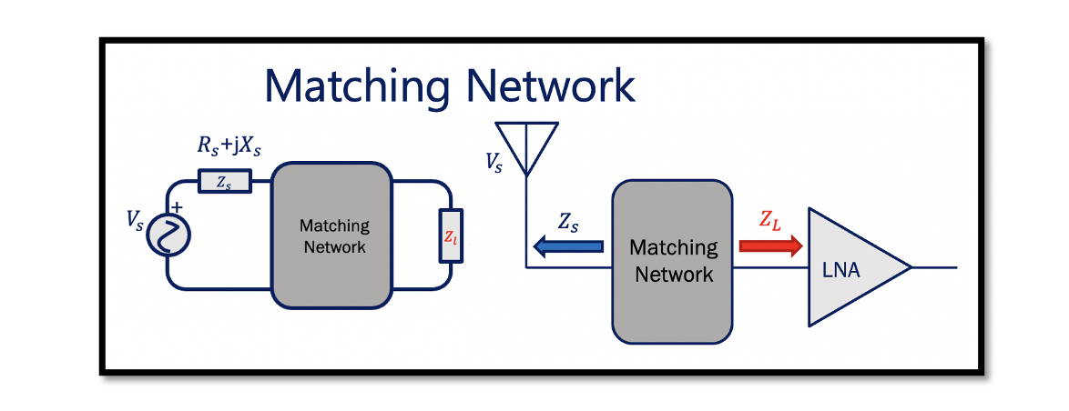

Maximum power delivery is the main objective while designing a circuit in RF systems and the purpose of creating matching networks is to maximise the power transfer with very minimum loss.The diagram shows the antenna and Low Noise Amplifier (LNA) blocks. Here, Zl is the input impedance of the LNA, and Zs is the output impedance of the antenna, which is mostly 50 ohms. As we read before in the maximum power concept that to have maximum power transfer in a circuit, the load impedance Zl must be matched to the complex conjugate of the source impedance Zs*. In order to follow this, the design of the LNA have to be altered to match, which is not acceptable. Changing the design of any blocks within the RF system result in change of specification for which the particular block is designed.
For example, in this case, the LNA design has a transistor along with capacitance; hence, the input impedance to this circuit would be 1/jcw, which is an imaginary reactance value. It is not possible to get maximum power as we cannot match an imaginary value to 50 ohm load impedance. Hence, now the case is that we have to deliver maximum power without altering the design of LNA and without changing the input impedance to the LNA. The question arises that how we can have maximum power delivered without altering the circuits of the devices in the block.
The solution is, we can do this by using matching networks to deliver maximum power without changing any designs of the blocks. We need a matching network between them to have maximum power transfer from the antenna to the Low Noise Amplifier (LNA). This matching network transforms the load impedance into a complex conjugate of the source impedance (Zl =Zs*), which is the maximum power transfer requirement.
As shown above, the matching network divides the circuit into two parts, the source, and the load. This matching circuit can be between any two blocks of RF systems, for example, between antenna and LNA, or between the filter and LNA. The matching network transforms the impedance into its input as the conjugate of the source impedance. So when we design a matching circuit as shown here, our matching network’s input will be the conjugate of the source impedance (Zs*).
If we design in a way that our input impedance of the matching network is conjugate of source impedance, we can deliver the maximum power to the matching network. At the output of the matching network, we get a lossless power. All the power from the matching network goes into the load. Hence, to completely deliver the available power to the matching circuit’s input to the output of the load, the matching network has to be lossless. It is practically not 100% lossless as there is some acceptable amount of power loss (PL).
The matching network is always designed using the reactive elements like inductance, and capacitance (L and C). The matching network never includes resistance, as it absorbs the average power. Read about complex power, and conjugate.
Here, shown are the input and output equivalent circuits for matching networks. The matching circuit’s input impedance (Zin) is equal to conjugate of source impedance (Zin=Zs*). If, Zs=a+bj then Zin= a-bj. By designing the matching circuit, we are trying to transform Zl from output to the matching circuit’s input. Let Zl be c+bj then we are transforming a-bj to c+bj. In the output equivalent circuit, the matching network is designed so that Zout will be equal to the conjugate of load impedance (Zl*) that is transforming Zs to Zout.
Taking the example of antenna and LNA, in this circuit we have a matching network added in between to have maximum power transfer. So if the antenna has an output impedance of 50 ohms, the Zin for the matching circuit should be 50 ohms, and the input impedance (Zl) to the LNA should be a+bj, and the output impedance of the matching circuit will be a-bj.
In summary, we expect to design the matching circuit where the Zin = Zs* and Zout= Zl* and have complete power transfer from Zin to Zout with very minimum acceptable loss (PL).